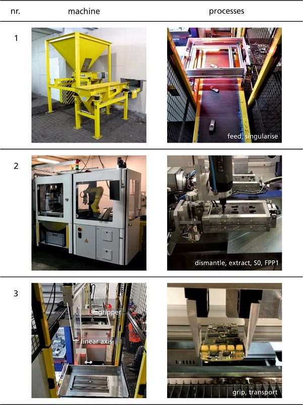
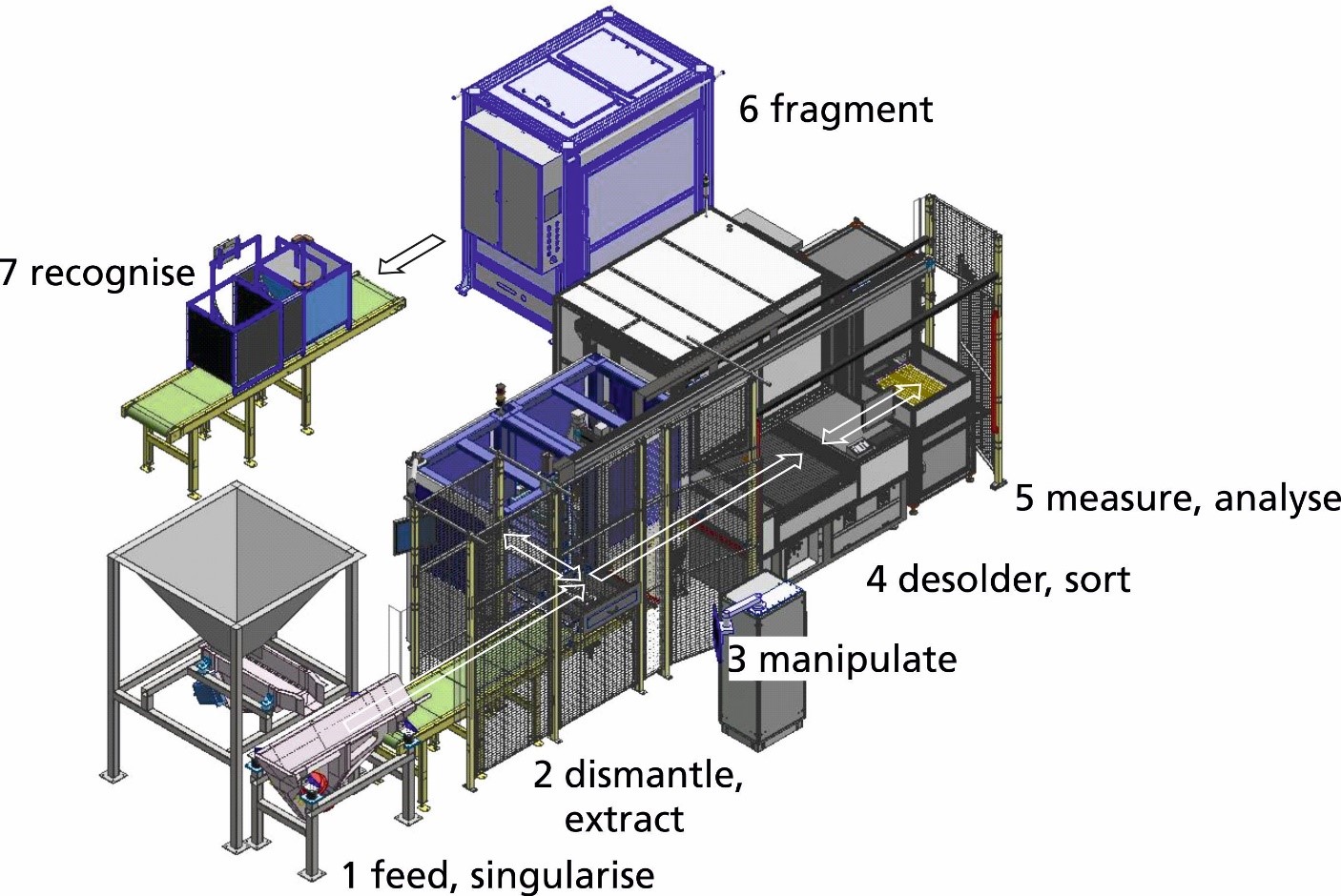
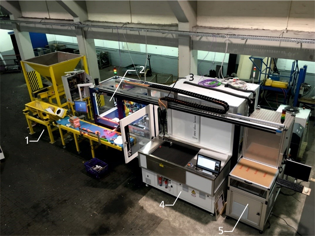
Based on these processes the worldwide first inverse production line comprised of seven machines was developed and set-up in a recycling plant of the consortium partner Electrocycling GmbH, in Goslar, Germany. The various machines and their functions are:
Machine 1 – feeding and singularisation,
Machine 2 – dismantling of MPHs, extraction of battery and PCB,
Machine 3 – manipulation of PCBs among the machines, loading/unloading actions,
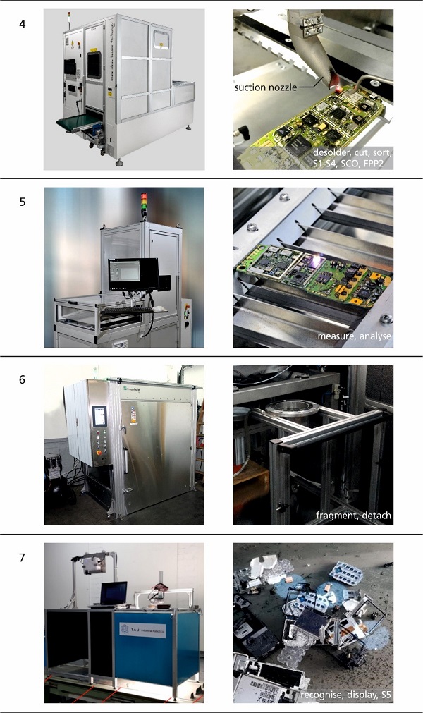
Machine 4 – desoldering, cutting out and sorting of electronic components,
Machine 5 – measurement of the 2D/3D geometry of PCBs and laser spectroscopic analyses,
Machine 6 – fragmentation of residues from MPH dismantling and processed PCBs,
Machine 7 – recognition of output of fragmentation machine 6 to identify vibration alerts.
© Fraunhofer ILT, Aachen, Germany. S0 sorting fraction for batteries, FPP1 fraction consisting of residues from MPH dismantling, provided for post-processing by machine 6.
© Fraunhofer ILT, Aachen, Germany. S1-S4 sorting fractions for desoldered electronic components, SCO sorting fraction for electronic components cut out from PCBs, FPP2 fraction consisting of PCBs processed by machine 4, provided for post-processing by machine 6.
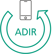
© Fraunhofer ILT, Aachen, Germany. ADIR demonstrator with seven machines.
The line of seven machines – called ADIR demonstrator – is able to work in two different operation modes: a) manual loading of PCBs (from MPHs or from servers) and then automatic handling as well as processing with machines 3-5, and subsequently with manual loading/unloading and automatic processing by machines 6 and 7; b) automatic loading, where mobile phones are conveyed and singularised from the feeding station to the dismantling station of machine 2; further processing as in a).
© Fraunhofer ILT, Aachen, Germany. Machines 1 to 5 during the installation phase at ECG, Goslar, Germany, Spring 2019.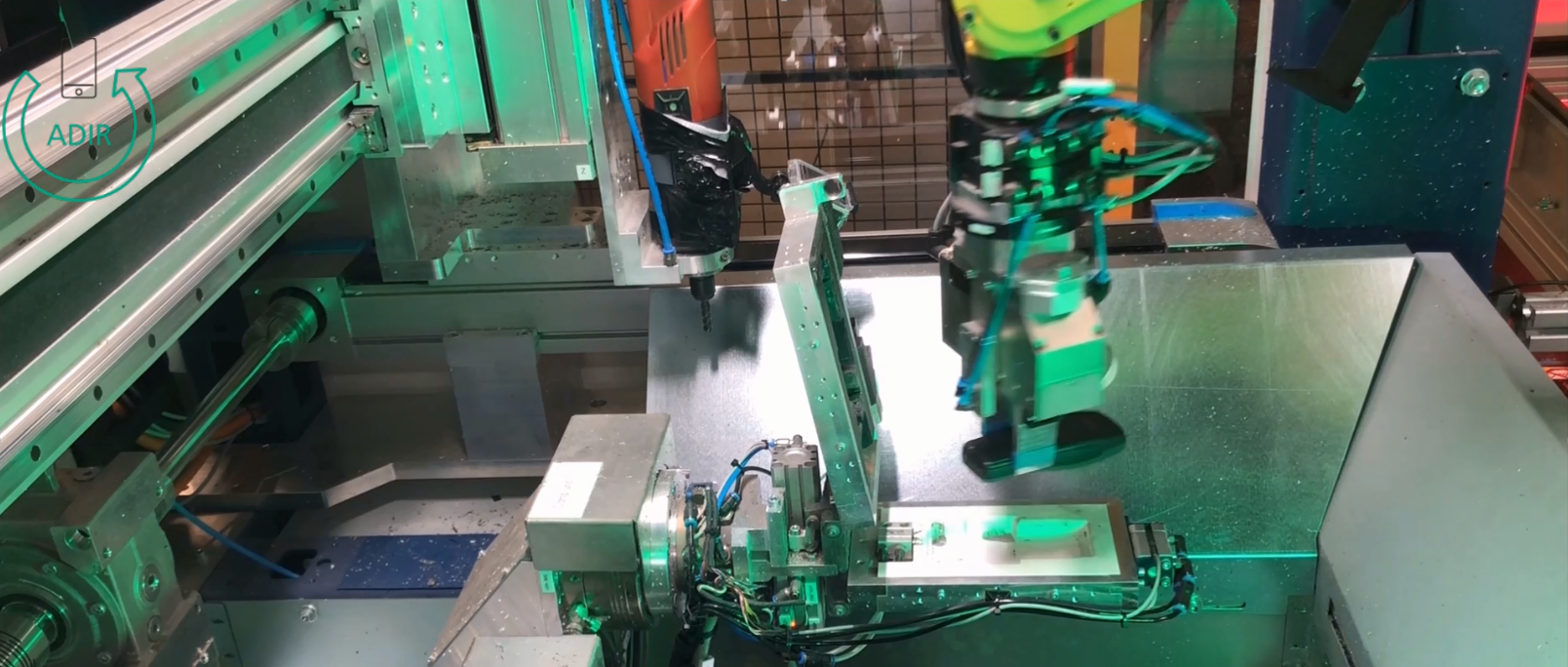
© Fraunhofer IFF, Magdeburg, Germany. A mobile phone gripped by a robot is loaded into a clamping unit for the disassembly of the MPH in machine 2.
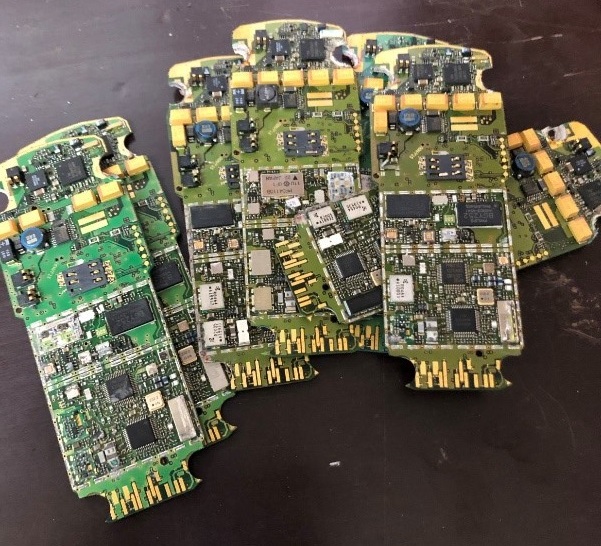
© Fraunhofer ILT, Aachen, Germany.Output of machine 2: printed circuit boards extracted from a mobile phone.
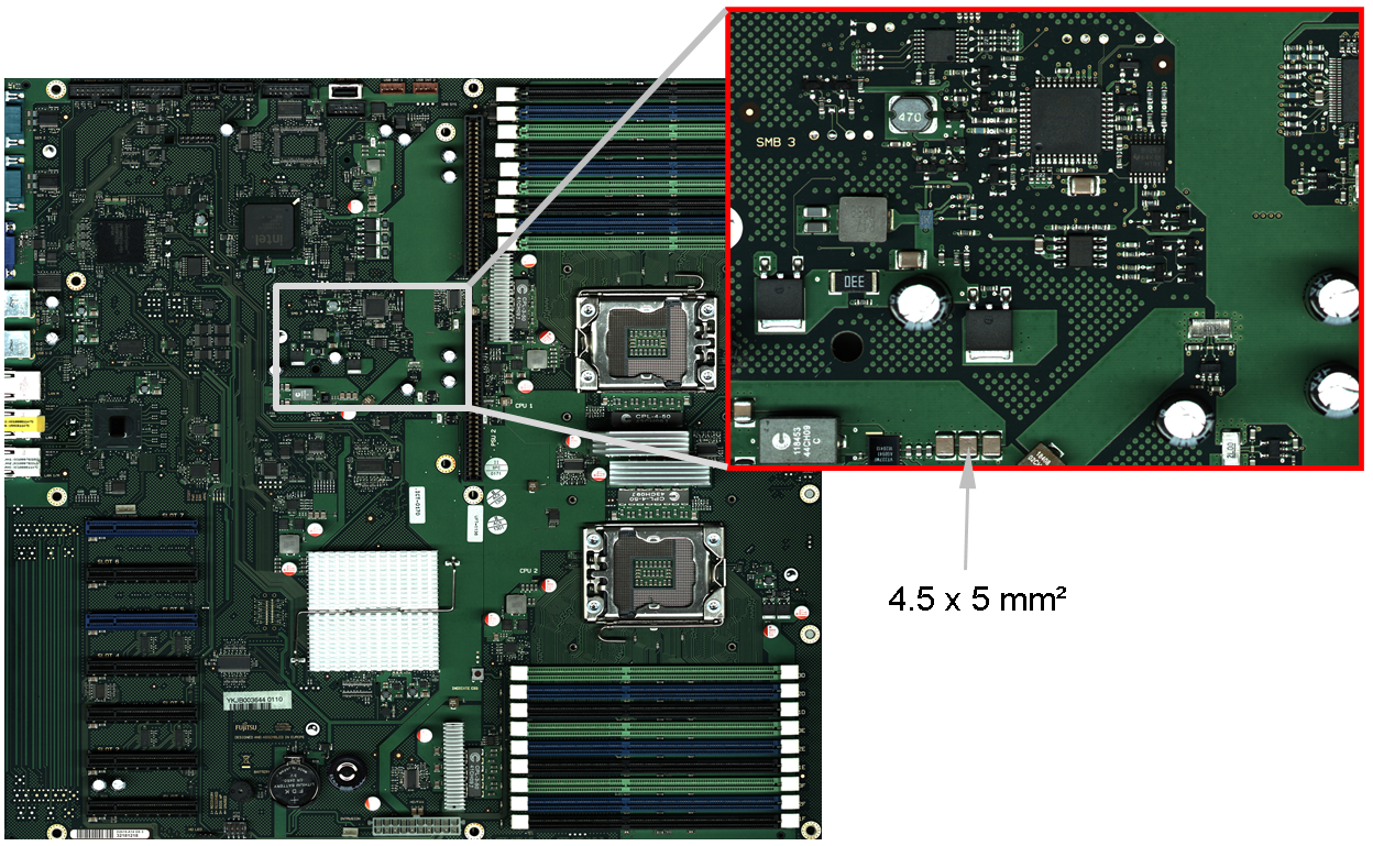
© Fraunhofer ILT, Aachen, Germany.2D high-resolution colour images of PCBs gained with machine 5 (spatial resolution 50 µm; full PCB image with up to 100 Mpixel). Right: enlarged view of rectangle shown on the left. Arrow indicates exemplarily a surface mounted device (SMD) with the dimensions 4.5 x 5 mm2.
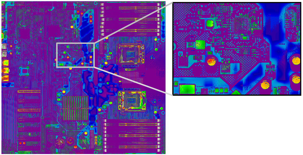
© Fraunhofer ILT, Aachen, Germany.3D high-resolution image gained by laser light section method in machine 5; height at each position of PCB is displayed as false colour. Right: enlarged view of rectangle shown on the left.
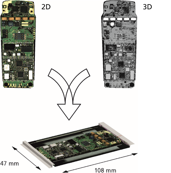
© Fraunhofer ILT, Aachen, Germany.Fusion of 2D and 3D images of a printed circuit board from a mobile phone to set-up a comprehensive geometric data set for PCBs in machine 5.
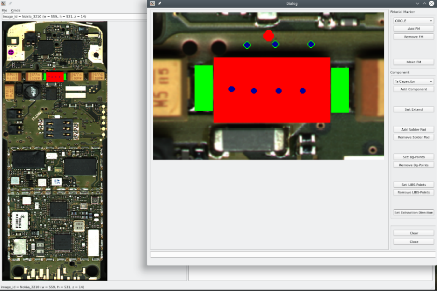
© Fraunhofer ILT, Aachen, Germany. Screenshot of the user interface to teach electronic components and to define the component list, which describes the set of electronic components, their positions, sizes and composition, to be desoldered in machine 4. The image on the left shows an example for the PCB of Nokia 3310. On the right the teaching of one component is exemplarily shown (red: body of electronic component, green: soldering pads, blue: measuring spots for laser spectroscopy).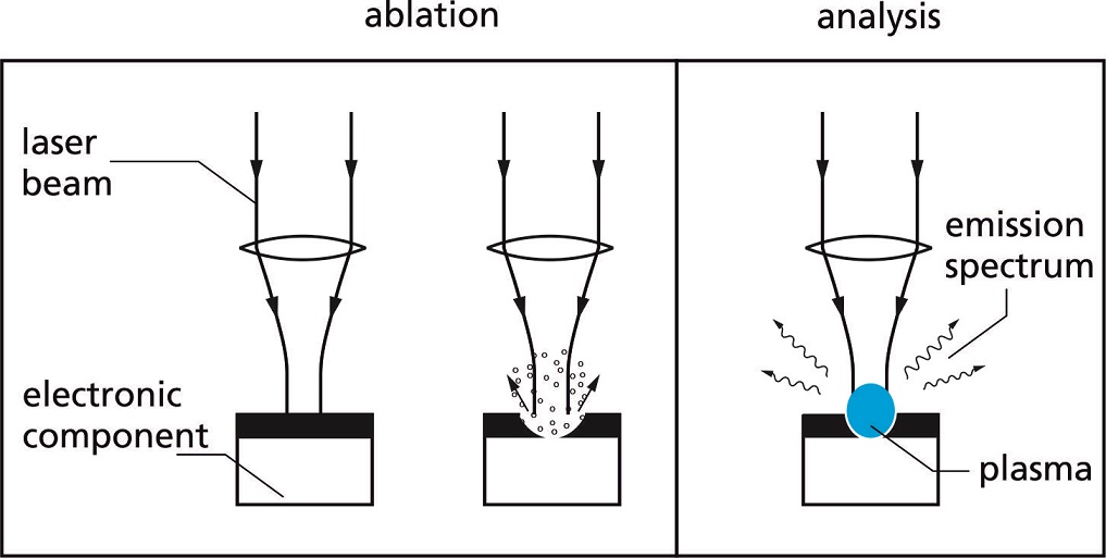
© Fraunhofer ILT, Aachen, Germany.Laser ablation of an electronic component to access the interior, such as e.g. the dielectrics of a capacitor with the valuable target material. Subsequently, the laser pulses induce a microplasmas to generate a spectroscopic signal to identify the target material. The laser spectroscopic method implemented in machine 5 is laser-induced breakdown spectroscopy (LIBS).
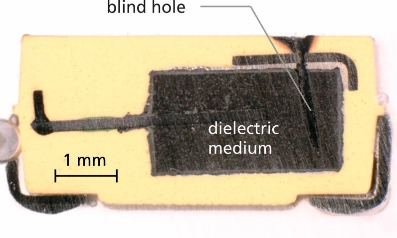
© Fraunhofer ILT, Aachen, Germany. Cross section of a tantalum capacitor. The arrow indicates the blind hole generated by laser ablation to access the dielectric medium.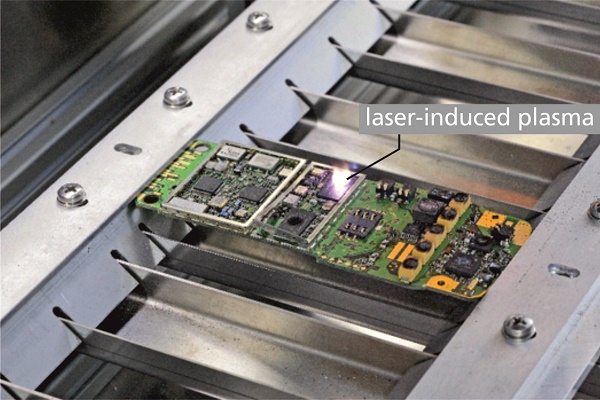
© Fraunhofer ILT, Aachen, Germany.Printed circuit board of a mobile phone clamped in machine 5 while a laser spectroscopic measurement at an electronic component is conducted, see bright spot of laser-induced plasma.
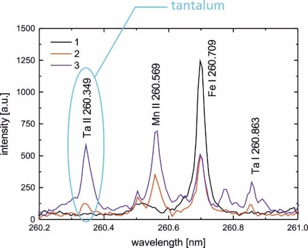
© Fraunhofer ILT, Aachen, Germany. Optical spectrum of a tantalum capacitor gained with laser spectroscopy. The black and red curves (1, 2) refer to measurements where the dielectric medium of the capacitor is not yet or only partly reached (blind hole is not deep enough), whereas the spectrum shown in blue (3) is gained after sufficient local ablation to reach the internal dielectric medium which is clearly indicated by the tantalum signal (emission line at ca. 260 nm).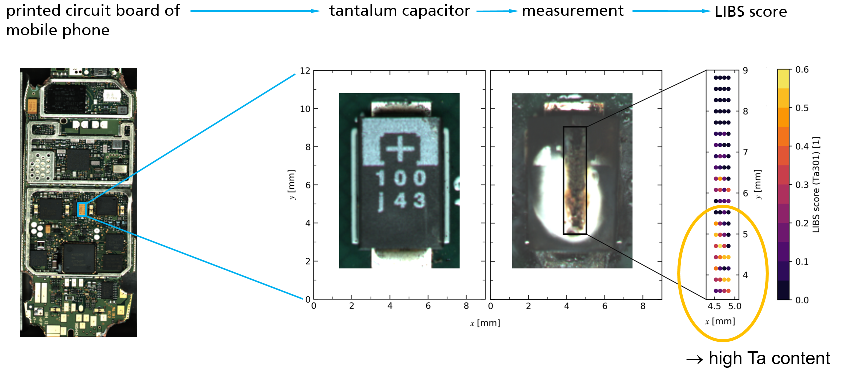
© Fraunhofer ILT, Aachen, Germany.Left: printed circuit board of a mobile phone; middle: tantalum capacitor prior and after the measurement in machine 5; right: LIBS scores indicating in yellow/red high tantalum content.
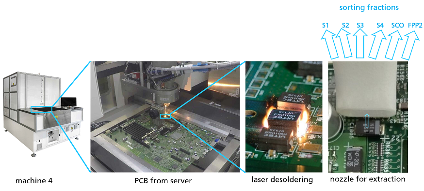
© Fraunhofer ILT, Aachen, Germany. Machine 4 for the selective desoldering of electronic components. S1-S4 sorting fractions of desoldered electronic components, SCO sorting fraction for electronic components cut out from PCBs, FPP2 fraction consisting of PCBs processed by machine 4, provided for post-processing by machine 6.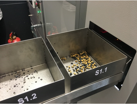
© Fraunhofer ILT, Aachen, Germany. Sorting fractions generated by machine 4. In the measuring campaigns conducted at ECG more than 1000 MPHs and more than 800 PCBs from servers were processed by the ADIR demonstrator. About 26 000 tantalum capacitors were automatically desoldered from PCBs using laser technology. Sorting fractions with the following enriched concentrations given in weight-% were gained: Ta 30-35 %, W 10-15 %, Nd >3 %, Au >0.15 %.
With novel hydrometallurgical processes high recovery rates were achieved with this input material: Ta 97.7 %, W 96 %, Nd 96 % Au >98 %.
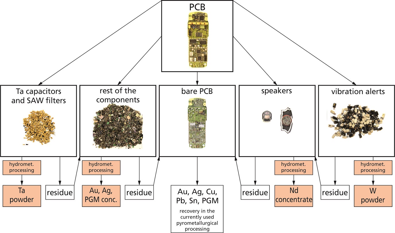
© Ł-IMN, Gliwice, Poland. Sorting fractions, hydrometallurgical (orange) and pyrometallurgical processes used for recovery of valuable materials. PGM platin group metals.
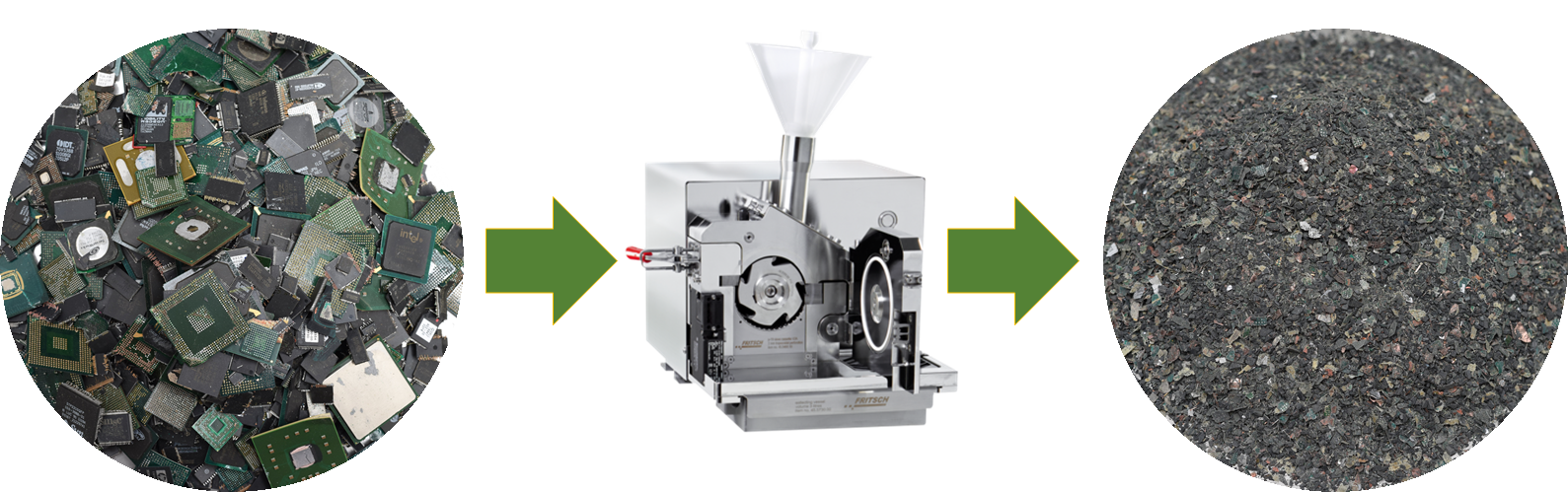
© Ł-IMN, Gliwice, Poland.Schematics of processing of sorting fractions; left: gold, silver and platin group metals fraction; middle: cutting mill, right: ground material. © Ł-IMN, Gliwice, Poland.
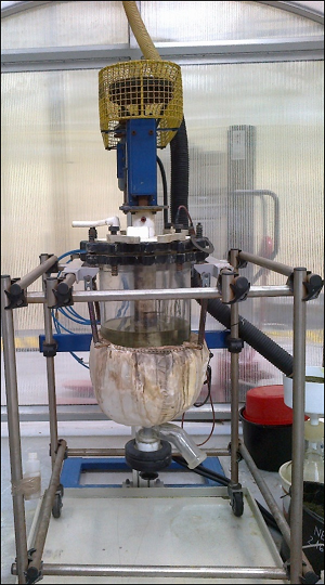
© Ł-IMN, Gliwice, Poland. Leaching reactor.
An economic estimate based on an assumed three-shift operation with machine hour rates of the process line in the order of 50 €/h, spans of market prices of raw materials of the last 3-5 years (min, max), showed that a break-even can be achieved for throughputs of the ADIR demonstrator of 300 MPHs per hour or 40 PCBs from servers per hour. For server PCBs this threshold is nearly reached with the ADIR machines. For MPHs processing times have to be further reduced significantly.
The consortium showed that via geometric measurements and spectroscopic analyses of EOL products, especially printed circuit boards, a selective dismantling and sorting is enabled. New return channels to production lines are opened. A first step to a data base for inverse production was made which is considered to be a key factor for sustainable recycling. The future vision is to define and implement a digital recycling pass for all industrial mass products. This pass shall provide – among others – information about the chemical constituents (elements, technology metals, …) as well as about procedures for selective dismantling and recovery.
Design for recycling demands are a key issue for future sustainable production:
– to simplify dismantling of complex electronic consumer products such as MPHs,
servers, personal computers, electronic appliances,
– to enable repair/exchange actions for components, modules, batteries.
This implies demands on joining technologies deployed for such appliances, their mechanical structures (radio frequency shieldings, mounting frames, …), composite materials, adhesives, etc. In future, the EU legislation should also refer to these topics as stated: recycling pass, design for recycling, share of recycled parts in new products as well as lifetime, sustainability, repairability (effort for repair actions, costs of repair pieces, exchange of energy storage media).
The consortium recommends to establish frame conditions in the European Union for the verification of the export stop of EOL-electronics out of the EU. Furthermore, regulations should be worked out to define stepwise increasing shares of secondary material from EOL-electronics to be refed into the production chain which goes beyond the usually considered overall mass fractions and includes strategically important technology metals as well.